- 您现在的位置:买卖IC网 > Sheet目录3818 > PIC18F4620-I/ML (Microchip Technology)IC MCU FLASH 32KX16 44QFN
1996 Microchip Technology Inc.
DS30412C-page 91
PIC17C4X
13.2.2
USART ASYNCHRONOUS RECEIVER
The receiver block diagram is shown in Figure 13-4.
The data comes in the RA4/RX/DT pin and drives the
data recovery block. The data recovery block is actually
a high speed shifter operating at 16 times the baud
rate, whereas the main receive serial shifter operates
at the bit rate or at FOSC.
Once asynchronous mode is selected, reception is
enabled by setting bit CREN (RCSTA<4>).
The heart of the receiver is the receive (serial) shift reg-
ister (RSR). After sampling the stop bit, the received
data in the RSR is transferred to the RCREG (if it is
empty). If the transfer is complete, the interrupt bit
RCIF (PIR<0>) is set. The actual interrupt can be
enabled/disabled
by
setting/clearing
the
RCIE
(PIE<0>) bit. RCIF is a read only bit which is cleared by
the hardware. It is cleared when RCREG has been
read and is empty. RCREG is a double buffered regis-
ter; (i.e. it is a two deep FIFO). It is possible for two
bytes of data to be received and transferred to the
RCREG FIFO and a third byte begin shifting to the
RSR. On detection of the stop bit of the third byte, if the
RCREG is still full, then the overrun error bit,
OERR (RCSTA<1>) will be set. The word in the RSR
will be lost. RCREG can be read twice to retrieve the
two bytes in the FIFO. The OERR bit has to be cleared
in software which is done by resetting the receive logic
(CREN is set). If the OERR bit is set, transfers from the
RSR to RCREG are inhibited, so it is essential to clear
the OERR bit if it is set. The framing error bit
FERR (RCSTA<2>) is set if a stop bit is not detected.
13.2.3
SAMPLING
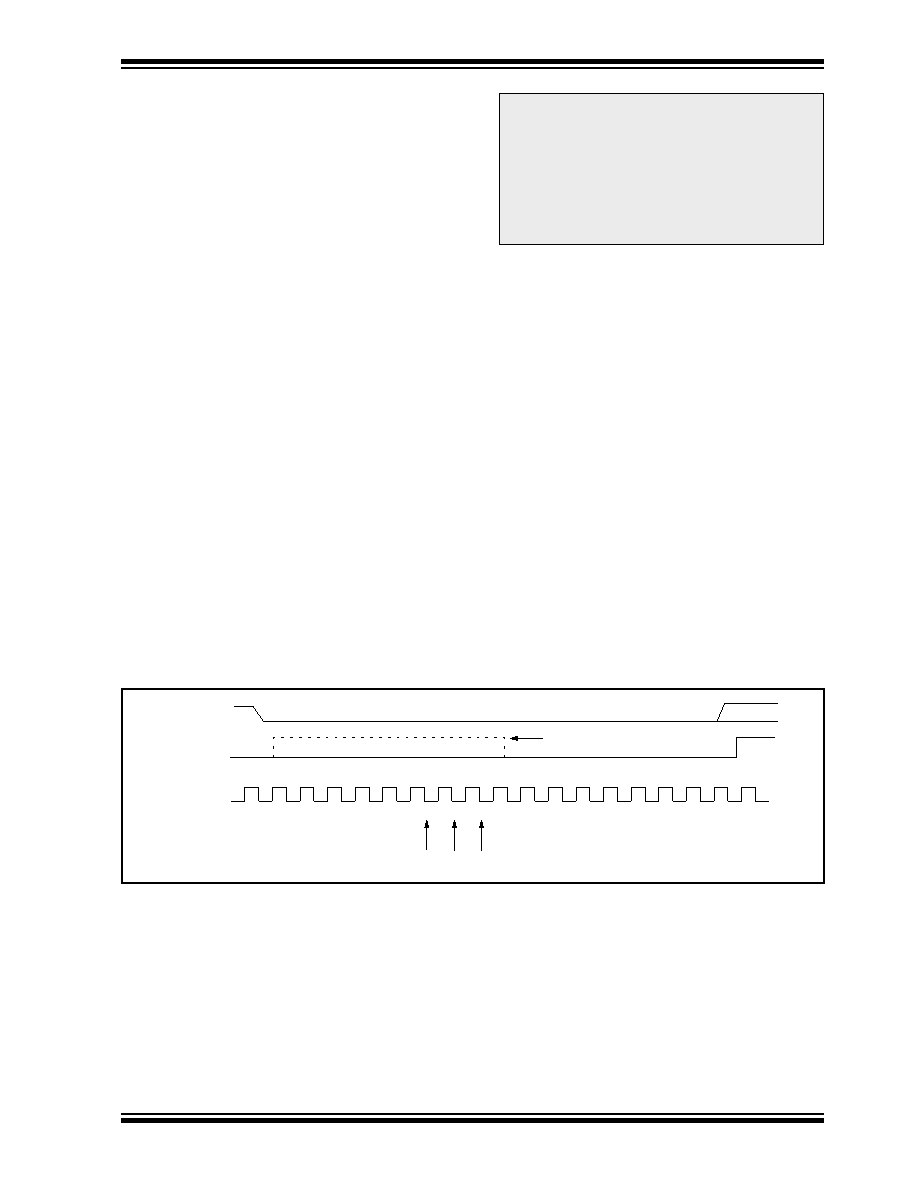
The data on the RA4/RX/DT pin is sampled three times
by a majority detect circuit to determine if a high or a
low level is present at the RA4/RX/DT pin. The sam-
pling is done on the seventh, eighth and ninth falling
edges of a x16 clock (Figure 11-3).
The x16 clock is a free running clock, and the three
sample points occur at a frequency of every 16 falling
edges.
Note:
The FERR and the 9th receive bit are buff-
ered the same way as the receive data.
Reading the RCREG register will allow the
RX9D and FERR bits to be loaded with val-
ues for the next received Received data;
therefore, it is essential for the user to read
the
RCSTA
register
before
reading
RCREG in order not to lose the old FERR
and RX9D information.
FIGURE 13-7: RX PIN SAMPLING SCHEME
RX
baud CLK
x16 CLK
Start bit
Bit0
Samples
1
2
3
4
5
6
7
8
9
10
11
12
13
14
15
16
1
2
3
Baud CLK for all but start bit
(RA4/RX/DT pin)
发布紧急采购,3分钟左右您将得到回复。
相关PDF资料
PIC24HJ256GP210-I/PT
IC PIC MCU FLASH 128KX16 100TQFP
PIC24HJ128GP310A-I/PF
IC PIC MCU FLASH 128KB 100-TQFP
DSPIC33FJ128GP310-I/PF
IC DSPIC MCU/DSP 128K 100TQFP
PIC16C66-20I/SO
IC MCU OTP 8KX14 PWM 28SOIC
DSPIC33FJ128MC510-I/PT
IC DSPIC MCU/DSP 128K 100TQFP
PIC16C66-20I/SP
IC MCU OTP 8KX14 PWM 28DIP
PIC18LF2620-I/SP
IC MCU FLASH 32KX16 28SDIP
PIC16F877-04I/P
IC MCU FLASH 8KX14 EE 40DIP
相关代理商/技术参数
PIC18F4620-I/P
功能描述:8位微控制器 -MCU 64KB 3968 RAM 36 I/O RoHS:否 制造商:Silicon Labs 核心:8051 处理器系列:C8051F39x 数据总线宽度:8 bit 最大时钟频率:50 MHz 程序存储器大小:16 KB 数据 RAM 大小:1 KB 片上 ADC:Yes 工作电源电压:1.8 V to 3.6 V 工作温度范围:- 40 C to + 105 C 封装 / 箱体:QFN-20 安装风格:SMD/SMT
PIC18F4620-I/P
制造商:Microchip Technology Inc 功能描述:IC 8BIT FLASH MCU 18F4620 DIP40
PIC18F4620-I/PT
功能描述:8位微控制器 -MCU 64KB 3968 RAM 36 I/O RoHS:否 制造商:Silicon Labs 核心:8051 处理器系列:C8051F39x 数据总线宽度:8 bit 最大时钟频率:50 MHz 程序存储器大小:16 KB 数据 RAM 大小:1 KB 片上 ADC:Yes 工作电源电压:1.8 V to 3.6 V 工作温度范围:- 40 C to + 105 C 封装 / 箱体:QFN-20 安装风格:SMD/SMT
PIC18F4620-I/PT
制造商:Microchip Technology Inc 功能描述:IC 8BIT FLASH MCU 18F4620 TQFP44
PIC18F4620T-I/ML
功能描述:8位微控制器 -MCU 64KB 3968 RAM 36 I/O RoHS:否 制造商:Silicon Labs 核心:8051 处理器系列:C8051F39x 数据总线宽度:8 bit 最大时钟频率:50 MHz 程序存储器大小:16 KB 数据 RAM 大小:1 KB 片上 ADC:Yes 工作电源电压:1.8 V to 3.6 V 工作温度范围:- 40 C to + 105 C 封装 / 箱体:QFN-20 安装风格:SMD/SMT
PIC18F4620T-I/PT
功能描述:8位微控制器 -MCU 64KB 3968 RAM 36 I/O RoHS:否 制造商:Silicon Labs 核心:8051 处理器系列:C8051F39x 数据总线宽度:8 bit 最大时钟频率:50 MHz 程序存储器大小:16 KB 数据 RAM 大小:1 KB 片上 ADC:Yes 工作电源电压:1.8 V to 3.6 V 工作温度范围:- 40 C to + 105 C 封装 / 箱体:QFN-20 安装风格:SMD/SMT
PIC18F4680-E/ML
功能描述:8位微控制器 -MCU 64KB 3328 RAM w/ECAN RoHS:否 制造商:Silicon Labs 核心:8051 处理器系列:C8051F39x 数据总线宽度:8 bit 最大时钟频率:50 MHz 程序存储器大小:16 KB 数据 RAM 大小:1 KB 片上 ADC:Yes 工作电源电压:1.8 V to 3.6 V 工作温度范围:- 40 C to + 105 C 封装 / 箱体:QFN-20 安装风格:SMD/SMT
PIC18F4680-E/P
功能描述:8位微控制器 -MCU 64KB 3328 RAM w/ECAN RoHS:否 制造商:Silicon Labs 核心:8051 处理器系列:C8051F39x 数据总线宽度:8 bit 最大时钟频率:50 MHz 程序存储器大小:16 KB 数据 RAM 大小:1 KB 片上 ADC:Yes 工作电源电压:1.8 V to 3.6 V 工作温度范围:- 40 C to + 105 C 封装 / 箱体:QFN-20 安装风格:SMD/SMT